|
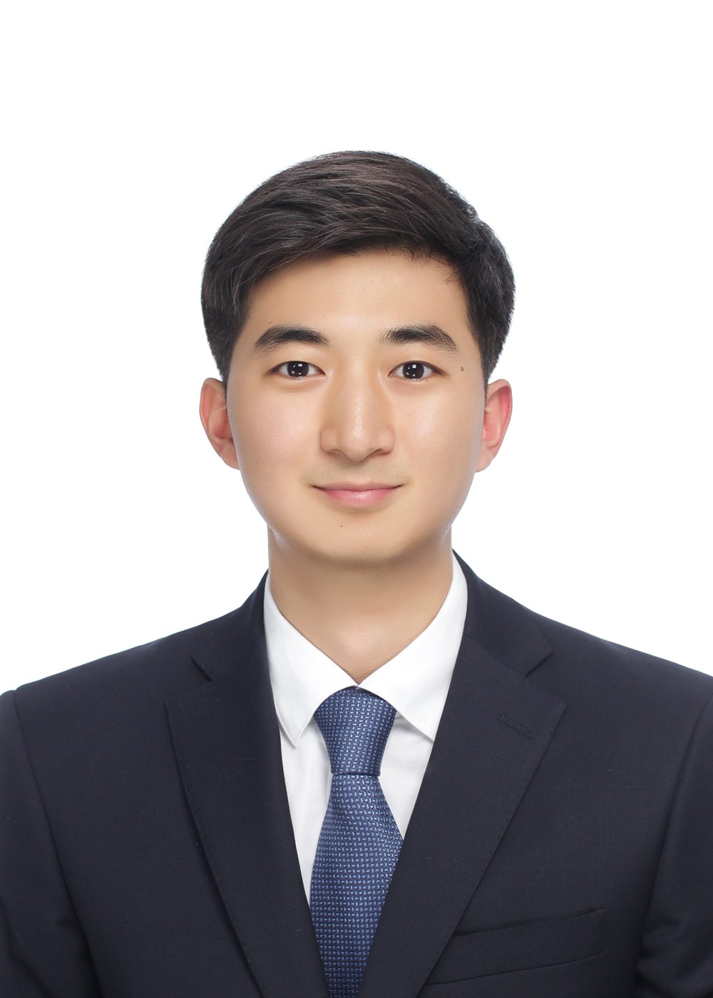
Seongwon (Gabriel) Yoon I am a Ph.D. student in Electrical and Computer Engineering at Georgia Tech, advised by Prof. Shimeng Yu in the Laboratory for Emerging Devices and Circuits. My research focuses on optical switch and interconnect co-design with silicon photonics for scalable AI systems. I received my B.S. in Materials Science and Engineering from Seoul National University, Summa Cum Laude. |
|
Research InterestsMy research focuses on silicon photonics and optical interconnects for AI infrastructure. I study how photonic integrated circuits (PICs) can replace copper across the scale-up and scale-out hierarchy of AI clusters, including co-packaged optics (CPO), near-packaged optics, and optical interconnects. On the system side, I work on optical link modeling and cross-layer analysis of power, thermal tuning overhead, and performance for large-scale LLM training. On the device side, I explore CMOS-compatible emerging devices such as ferroelectrics and oxide transistors for photonic–electronic integration, along with modulator and transceiver device physics. Keywords: Silicon Photonics, Optical Interconnects, Optical Device Modeling, AI Infrastructure Publications |
|
An Optical KV Cache Network for Disaggregated LLM Serving
Seongwon Yoon, Shimeng Yu arXiv preprint arXiv:2610.18444, 2026. [pdf] |
|
Cross-Layer Analysis of Thermal Tuning Stalls in Wafer-Scale Optical Interconnects for LLM MoE Training
Seongwon Yoon, Pin-Jun Chen, Shimeng Yu arXiv preprint arXiv:2608.24637, 2026. [pdf] |
|
CMOS+X: Stacking Memories based on Oxide Transistors upon GPGPU Platforms
Faaiq Waqar, Ming-Yen Lee, Seongwon Yoon, Seongkwang Lim, Shimeng Yu Proceedings of the International Symposium on Memory Systems (MEMSYS), pp. 64–77, 2025. [pdf] |
|
A CMOS Image Sensor Pixel Readout Circuit Design Using Back-End-of-Line (BEOL)-Compatible Oxide Transistors
Seongwon Yoon, Janak Sharda, Omkar Phadke, Shimeng Yu IEEE 68th International Midwest Symposium on Circuits and Systems (MWSCAS), pp. 1026–1030, 2025. (Best Paper Award) [pdf] |
|
Solving Max-Cut Problem Using Spiking Boltzmann Machine Based on Neuromorphic Hardware with Phase Change Memory
Yu Gyeong Kang, Masatoshi Ishii, Jaeweon Park, Uicheol Shin, Suyeon Jang, Seongwon Yoon, Mingi Kim, Atsuya Okazaki, Megumi Ito, Akiyo Nomura, Kohji Hosokawa, Matthew BrightSky, Sangbum Kim Advanced Science, vol. 11, no. 46, 2406433, 2024. [pdf] |
|
Clinical Validity and Precision of Deep Learning-Based Cone-Beam Computed Tomography Automatic Landmarking Algorithm
Jungeun Park, Seongwon Yoon, Hannah Kim, Youngjun Kim, Uilyong Lee, Hyungseog Yu Imaging Science in Dentistry, vol. 54, no. 3, pp. 240–250, 2024. [pdf] |
|
Solving Constraint Satisfaction Problem with Spiking Neural Network based on 1.4M 6T2R PCM Synaptic Array with 1.6K Stochastic LIF Neurons Neuromorphic Hardware
Seongwon Yoon, Uicheol Shin, Sangbum Kim The 28th Korean Conference on Semiconductors (KCS), 2021. [pdf] |
Chip Tapeout |
|
RRAM-Integrated CMOS Image Sensor Pixel Readout Chip
180 nm CMOS, 3-metal MPW through the National NanoFab Center (NNFC), Korea Laboratory for Emerging Devices and Circuits, Georgia Tech, 2025. |
Talks |
|
Optical Interconnect for LLM, MoE and Agentic AI
Future of CMOS and Talent Workshop, Session 2: Memory Wall and Interconnect Wall Georgia Tech Global Learning Center, Atlanta, GA, March 26, 2026. |
SkillsPhotonic & Electromagnetic Simulation: Ansys Lumerical (FDTD, MODE, INTERCONNECT) Device & Multiphysics Simulation: TCAD, Ansys Mechanical (thermal and structural analysis) Scientific Computing: MATLAB |
Graduate CourseworkCourses taken at Georgia Tech. Networking
VLSI & Semiconductor Devices
Computer Architecture & ML Systems
Machine Learning & AI
|
|
Design and source code from Jon Barron Website. |